I took pictures of taking apart my i-opener so I could share what I've
learned, as well as to provide a roadmap for taking it apart later. I hope
that I can make things easier for others interested in modifying their
boxes. For good instructions on opening your i-opener, visit Adam's
Guide to the i-opener. I'm not a hardware guy: I mostly do software,
so bear with my descriptions.
Here, in rough chronological order, are i-opener images. These are thumbnails:
each leads to a higher resolution (though maybe no less fuzzy) image. It's
too bad that I don't have more detail: blame the digital camera and the
incandescent light I was forced to use.
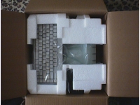 |
The i-opener in the box. 4.67 kg in original packaging with documentation.
Here, the documentation (a large sheet explaining installation, a yellow
paper explaining how to set up network service, and a 20 page manual) have
been removed. The keyboard is mounted above the i-opener proper, and is
already connected. There is a wall mounted transformer and RJ-11 telephone
cable, as well. |
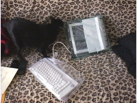 |
Pyewacket checks out the i-opener. It's new, cool, and his size. He
likes it. |
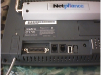 |
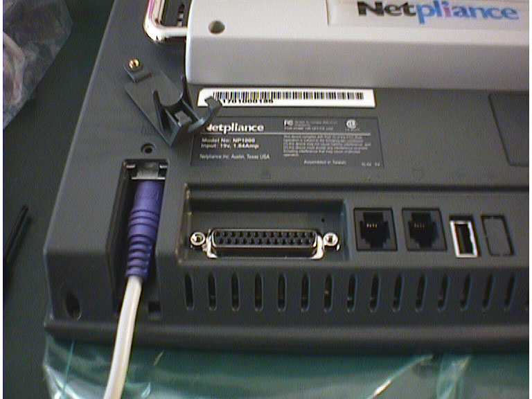
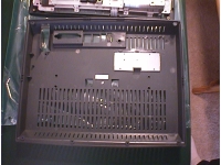
The back of the i-opener. No, you can't really read the serial number
of details in this photo. Notice how the keyboard plug is protected against
removal by the secured sliding latch. Also, to the right of the photo,
you can see half the flash ram cover--this is replacable in the field.
You need to have long nails or thin fingers to remove this hatch easily. |
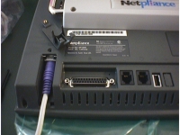 |
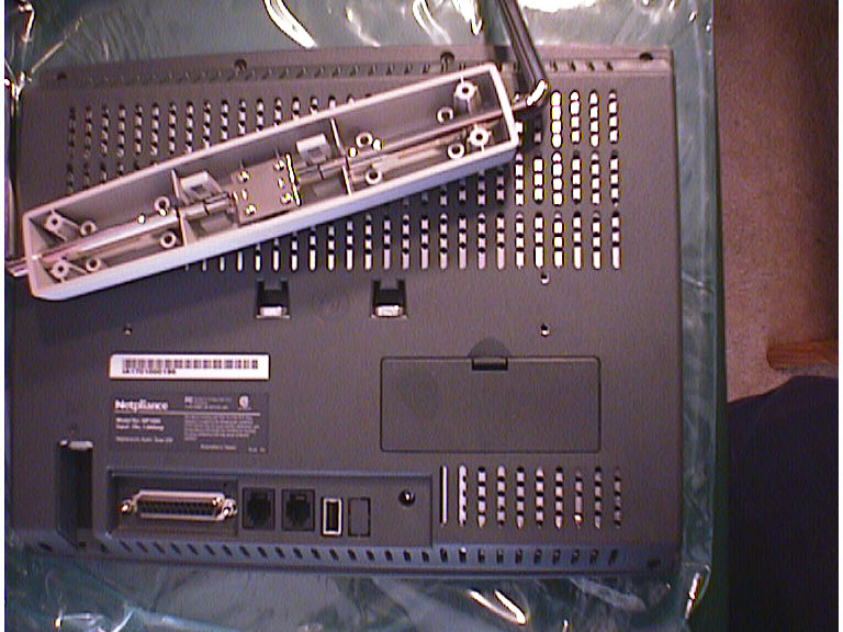
The sliding latch over the keyboard plug has been removed. No fancy
soldering or tricks required. You can probably read some of the words in
the nameplate in the large version of this image. |
 |
I removed the stand before trying to remove the back. I wasn't sure
if the stand was secured to the RF shield, but I didn't want to take chances.
Also, I figured the stresses imposed on the plastic back would be lessened
if I removed the heavy metal stand first. Note that only four screws hold
the stand in place--these (and one small screw and two bolts) are the only
non-standardized screws in the installation. Every other screw on the i-opener
is identical. Also, note the tabs that hold the stand and i-opener together.
To make removing the stand easier, slide it down slightly before removing
it so you don't damage or stress the tabs and slots. |
 |
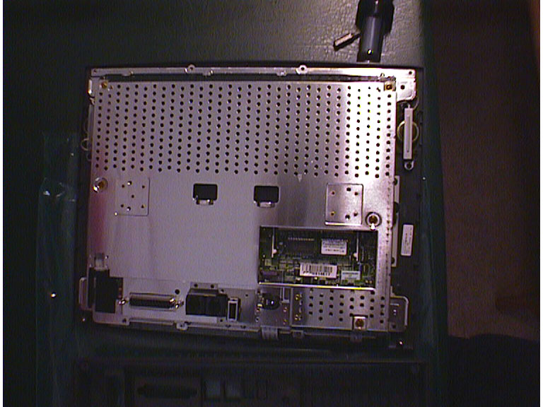
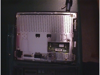
The inside of the back of the plastic cover. The most difficult part
of removing the plastic cover is popping the plastic snap-tabs. The top
of the back cover has four screws holding it in place, with two additional
screws at the bottom. The sides are each held in place with a plastic snap
in the center, and at the bottom, two plastic snaps hold the bottom on.
Notice the RF shielding over the memory slot, and the white sticker in
the center. Each major piece has one of these "Foxcom" stickers with a
manufacture date (mine was in January 2000).
|
 |
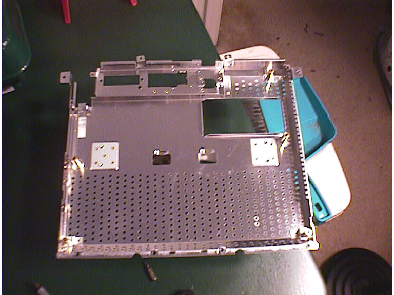
The outside of the RF shield. Of special note are all the rivets and
patches of aluminum used in high stress areas: where the stand attaches
to the shield, around the USB jack, on the top of the RJ-11 jacks, and
beside the power plug. |
 |
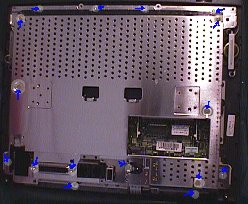
I've identified the screws that need to be removed to remove the RF
shield. Double check that you've removed them all. The shield comes off
fairly easily--if you feel any significant resistance, you missed a screw.
Note that the bottom of the RF shield is bent near the bottom two screw
holes to lock the shield against the casing, and that additional material
has been bent to provide support for the RJ-11 jacks and the USB port--these
make a snug fit. The RF shield serves a dual purpose: blocking radio interference,
and grounding the system. Note that the two printer lugs and the very small
screw next to the power plug need to be removed before the shield can be
removed. |
 |
The inside of the RF shield. You can easily see the added metal to
support the stand, as well as the rivet holes for the additional metal
to reinforce the USB port and RJ-11 jacks. |
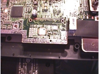 |
I was interested in the flash adapter. I was disappointed to find that
there is no hardware present, though the pattern and connectors are in
place. Notice the attachment holes for a flash socket to be mounted, as
well as the solder or tin around the edge of the board. This touches the
RF shield for grounding. |
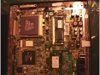 |
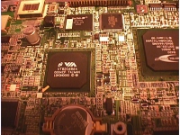
A (fuzzy) overview of the other half of the motherboard. Notice the
CPU, Cyberblade PCI-bridge and video IC, and the memory socket. Above the
memory socket, notice the second serial port and the dip switches. |
 |
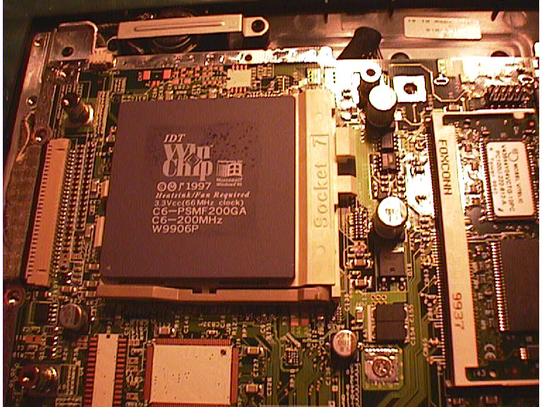
Detail of the CPU. This tells me that this is a 66MHz bus machine,
200MHz processor (yeah!), and regular socket 7 plug. You can see a speaker
mount and jack above the CPU, and the LCD connection (braided wire shield)
to the left. To the right is the memory. Below the CPU you can see unused
chip mounts.
|
 |
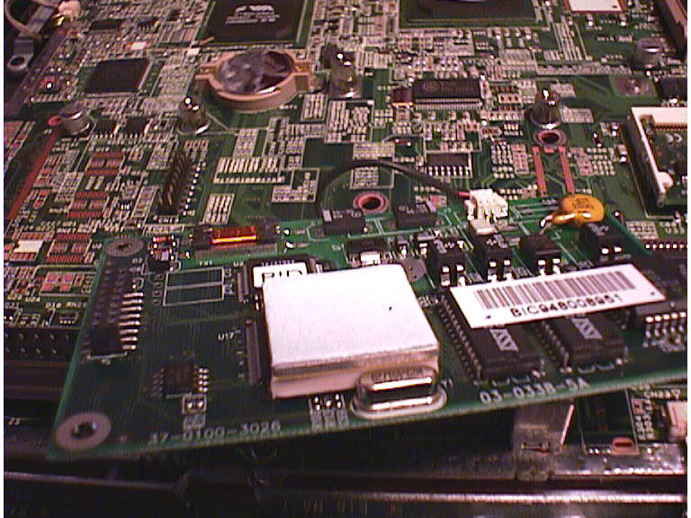
A close-up of the VIA chipset and SanDisk chips. This isn't a terribly
sharp photo, but you can also see a transformer in the upper left, and
a battery (Maxell dated "99") below the VIA chipset.
|
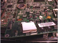 |
I carefully removed the modem from the first serial port adapter. It's
a typical, albeit small, socket. Notice the shielding around a chip on
the modem--I didn't bother removing it or the sticker over the two chips
to the right. A black and red wire connects from the modem daughterboard
to a socket on the motherboard.
|
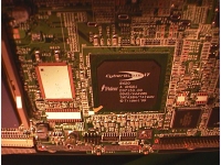 |
Detail of the Cyberblade chip. Also, you can see to the bottom of the
image the resistors and back side of the mail and phone LEDs. Worrywarts
note that I have an IDE plug and VGA plug.
|
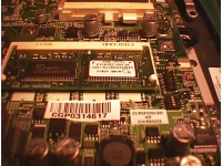 |
Detail of the memory, second serial port, and dip switches. Note the
position of all the switches--this is the same as in other pictures from
other i-openers. Notice that I have a white sticker below the memory--I've
seen yellow in other i-openers. |
More pictures will be forthcoming when I get my conversion kit. And,
no, I haven't plugged it in yet. I'm going to try to get a virgin flash
image via Linux.
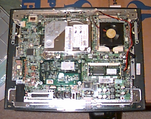
A picture of the completed job is below. And, surprisingly, everything works just
fine...except the Linux Kernel 2.4, which doesn't like booting. I'm thinking I might
just decide to go with Win98 on the box, anyway, mostly because this is going to be
a low-end client for the living room.